Undervolting GCN, Now Updated to GCN 5 (Vega)

This is mostly me updating a guide I wrote a while back for GCN. This means this is mostly copy,paste and edit with the exception of including steps for Polaris and Vega.

Introduction

Following this http://www.tomshardware.com/reviews/msi-afterburner-undervolt-radeon-r9-fury,4425.html I have decided to write a guide on undervolting AMD GPU’s. This guide will cover the first and second generation of the GCN architecture, although it should apply to third gen too (Tonga and Fiji).

Following this http://www.tomshardware.com/reviews/msi-afterburner-undervolt-radeon-r9-fury,4425.html I have decided to write a guide on undervolting AMD GPU’s. This guide will cover the first and second generation of the GCN architecture, although it should apply to third gen too (Tonga and Fiji). I am making this guide for that one guy who is curious and find this post by Google.

Reason to undervolt:

  • -reduced power consumption
  • -reduced fan noise from both GPU and PSU
  • -reduced load on PSU
  • -reduced temperatures
  • -provides a challenge by finding your cards absolute limits

Recommended Software Tools

For GCN 1/2
-VBE7 for Gen 1 GCN (Tahiti, Pitcairn and Cape Verde and their refreshes)
Download:http://www.techpowerup.com/forums/threads/vbe7-vbios-editor-for-radeon-hd-7000-series-cards.189089/
-HawaiiReader for Gen 2 GCN (Hawaii and Bonaire?)
Download:https://github.com/OneB1t/HawaiiBiosReader
From the thread:https://www.overclock.net/t/1561372/hawaii-bios-editing-290-290x-295×2-390-390x
-Hex editor for Gen 3 GCN (Will not be covered in this guide)
-GPU-Z
Download:https://www.techpowerup.com/downloads/2627/techpowerup-gpu-z-v0-8-7/
-Overclocking software
My recommendation:http://www.guru3d.com/files-details/msi-afterburner-beta-download.html
-Flashing program
https://www.techpowerup.com/downloads/2531/atiflash-2-71/ for the lazy people and https://www.techpowerup.com/downloads/2306/atiflash-4-17/ for USB users
I recommend following this guide for the ATIFLASH :https://www.techinferno.com/index.php?/forums/topic/1331-guide-amd-vbios-flashing/

For GCN 2-5 RECOMMENDED
-OverdrivenTool for Hawaii to Vega
Download:https://forums.guru3d.com/threads/overdriventool-tool-for-amd-gpus.416116/

In 2016, AMD introduced Wattman into the drivers. Since then AMD has improved on Wattman allowing much greater control for the end user. While the benefit does exist that it is possible to set individual profiles for every game, Wattman is not as practical as 3rd party tools. This is due to issues such as profiles not saving and not applying when the computer has started up. Due to this Wattman is not recommended.

Note:
A GPU with unlocked voltage control is necessary. This may not be possible for Gigabyte card’s as they have been locking down there voltages on a good portion of their AMD cards. An example would be the R9 280X Windforce.

Like overclocking when undervolting you are going to want a suitable components to work with. It is recommended you have a solid PSU that can provide consistent and clean power. A solid power supply refers to the build quality being competent when put under load. Recommend checking reviews done on johnyguru, techpowerup and tomshw.de. A poorly designed power supply can be similar to having a ticking time bomb for the rest of the components.

Voltage Curve

Below I have provided a Core Freq Vs Voltage Graph. This one in particular applies to Hawaii based chips and should not be used to for first gen GCN products or any products after due to changes in the node and architecture. This graph gives an idea at what voltage would be stable at any specific frequency especially when creating a power table. The graph with a ±30mV should be where actual minimum voltage be at any desired frequency when taking account manufacturing variances. This graph was made testing a ~70% percentile ASIC chip.

https://www.overclock.net/photopost/data/1483067/0/0d/0dcb8767_Untitled.png
Figure 1. A graph of what can be expected of a Hawaii GPU voltage/frequency curve.

Peak Efficiency of the GCN 1/2/3 Architecture

It has been known since the GCN introduction, that GCN up to Fiji is most efficient from the range between 800-900mhz on the core. The 7970 launched with a core speed of 925mhz. This is the area to maximize MHz/watt.

https://www.overclock.net/photopost/data/1483067/9/96/969ce4b4_Untitled2.png
Figure 2. Marking the part of the graph where a large gain in voltage is needed for minor gain in frequency.

Some More Data and Reasons

I have provided some measurements that I obtained from GPU-Z. The data is only as accurate as the sensors and software i used. These values were obtained for running Hitman:Absolution maxed out at 1080P for 10minutes. The GPU used is the MSI R9 390X. As we can see from the data the when I give up 20mhz and drop a solid 100mV the average power in drops by 50W and the max power in drops 60W. With less load variation the power supply does not need to work as hard. The temps drop slightly (as I used the default fan curve here) but the fan speed drops from 44% to 32%. This leaves a strong drop in noise making the card that much more quieter.

https://www.overclock.net/photopost/data/1483067/8/83/8366b2b9_Untitled3.png
Figure 3. Data based on testing done.

My test system at time of testing is as follows (Everything that is powered):

4770K @ 4.4Ghz 2.010VRIN 1.315V Core
32GB of GSkill Sniper 2400mhz 1.65V
Asus Z87-A
MSI GAMING OC R9 390X
Asus Xonar DS
512GB BX100
128GB M550
3TB WD Green 5200RPM
1TB Seagate 7200RPM
AX760
2 NF-F12
2 NF-A15
2 NF-A14 PWM
2 NF-A14 FLX
Mionix Naos 7000
MSI CK Black
Testing Procedure:
The game Far Cry 4 for two reasons. It is consistent in its load as staring at a fire inside the safehouse at the Royal Guard Kennels does not introduce random load variables to affect power draw. It is also very heavy on the CPU and GPU providing high usage on both ends.
Settings will be maxed out at 1440P with SMAA. INI edits were done by such as alpha to coverage quality.
The results of testing with power efficiency (PE) on and off are below.

https://www.overclock.net/photopost/data/1483067/0/02/0261d75e_imga.png
Figure 4. Testing the Power efficiency option in the AMD drivers for Hawaii.

As we see from here we can get quite excellent power consumption drop through undervolting.

The Power Efficiency Option

Based off the data from above it appears that the option doesn’t really do much. The option most likely works as it increases the polling rate at which powertune changes the voltages. Ideally this would mean the card would be able to downclock more quickly if there are instances idling to reduce the power consumption. I base this off the fact that adding “PP_AllGraphicLevel_DownHyst” to regedit at value to stopped any downclocking in crimson. That said PP most likely refers to powerplay and allgraphiclevel refers to the DPM states. With the downhyst referring to hysteresis the setting would affect how often the powertune checks to see if it should downclock to reduce power consumption. This option does not exist for Polaris onward and may have been removed some time ago.

Undervolting Auxiliary Voltage and its Effects

After dropping it by a whopping 131mV i have found that the power consumption does not change at all. This was done at a BIOS level. However when done on the software side such as MSI-AB, I noticed a drop of 7-8W. Not bad for -100mV. That said, don’t bother undervolting auxiliary because there are major stability issues if it is too low. Due to that it is can be considered not worth it due to the risks.

For Vega cards this option should be referred to as HBM voltage. This does not actually change the HBM’s voltage as those are hard set in the bios at 1.35V for Vega 64 and 1.2V for Vega 56. Functionally they do the same with the exception that “HBM voltage” will limit how low the core voltage may go. The core voltage for Vega may only go as low as what is set for “HBM voltage.”

On to the Actual Undervolting!

Requirements:
-A stressing app and time

It is advisable against using “apply overclock at startup” while stability testing. If the undervolt is unstable this can lead to the a constant boot cycle unless booted into safe mode as afterburner would no longer launch and adjustment can be made from there.

Like overclocking you will want to be looking for artifacts that occur. An artifact is very apparent when it occurs as the squares will appear completely out of place. Also be aware of the driver freezing/crashing/resetting. These symptoms occur due to instability, most likely due to too high frequency on the memory for GCN 1-4 and too low voltage for GCN 5(Vega) as Vega has ECC built into HBM2. The error-correcting code (ECC) in HBM2 makes it very difficult to see artifacts as they are corrected by ECC. This also makes testing for Vega more difficult. So, using your overclocking app you will want to follow this order:Drop the voltage->Check for instability->If fail decrease core frequency, if pass decrease the voltage again. This is a rinse and repeat process. I recommend dropping the voltage by 6.25mV intervals and the core by 10 or 5 MHz. The voltage controller AMD uses goes in 6.25mV intervals since Hawaii and presumably onward post GCN and is also used for the Zen motherboards.

Vega In Particular

With GCN 5, AMD has changed how powertune in particular works. Vega now takes into account several variables include: die temperature, fan speed, power consumption, voltage and GPU load. Before with the first 4 generations of GCN the core clock set was the core clock put out. With Vega this is not longer the case.

Figure 4. Example powerplay table

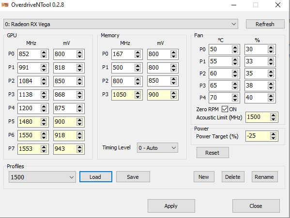
In Figure 4 the P7 state is set to 1553 MHz at 943mV. In Battlefield 1 the actual core clock ranges from 1505-1480 MHz with the “GPU Power” draw going from 160-180W respectively. The frequency also changes based on the load of what is occurring at that instance. The voltage fluctuates between 0.912-0.900V post Vdroop. It has been set to hard cap at 180W through the -25% power target hence the frequency throttling. When not throttling the core frequency is around 1500 ± 5 MHz. This is most case scenario. This is one of the disconnects with Vega, as what is set is not what is outputted and needs to be taken into consideration when tuning Vega. Due to this increasing the frequency by 10 MHz may not create a 10MHz increase in the actual core clock. As the GPU under load will be swapping between P7 and P6 are the main focus. Setting P5 and below should just be reasonable. If the load is too low like when playing a game like League of Legends then the stability of P5 and below may need to be tested. This is the one benefit of Wattman. It is possible in Wattman to select individual states by right clicking the state and set them as maximum either minimum state. Using this it is possible to test each state individually.

Notes:
When undervolting second gen GCN cards (Hawaii) you might find some stability by also dropping the memory clock as Hawaii has the memory tied to the core voltage.
Also if you set the voltage too low you may find instability on your 2D clocks. This is because second and third gen GCN cards use offset rather than a set voltage and when you have it applied it will affect all states. For example idle voltage is on the 390X is 0.9V. However if applying a -100mV offset it will hit 0.8V which may cause it to become unstable at desktop. There is a workaround called “Bios editing.” I do not recommend bios editing as the same can now be done with OverdriveNtool.

Using OverdriveNtool

OverdriveNtool is the most versatile tool made by a third party for AMD GPU’s. It allows for multiple profiles to be saved as well as saving the profile to the registry. This creates the capability to have 1 profile to be at 1500 MHz another at 1650 MHz, all up to the end user.

When running OverdriveNtool in administrator mode the PPtable editor can be accessed by right clicking the app. This opens the “SoftPowerPlay Table Editor” which allow saving of the settings in the registry. This avoids any necessity of modding the bios to save the settings. Bios modding is not possible with Vega GPU’s.

Bios Editing

Disclaimer:
I do not take any responsibility for any mistakes you make. When you do a bios edit you accept full responsibility on the chance you may make a mistake and brick your GPU. Also credit to gupstergs thread for making this part possible.

This only really applies to second and third gen GCN as you can have programs such as MSI AB apply your undervolt at startup for your first gen GCN card.
Once you find your desired frequency at X voltage I recommend you set it in bios for second and third gen GCN cards as this will allow a workaround for the offset. I will only be covering second gen here.

HawaiiReader

Exporting your stock bios is done VIA GPU-Z. This is done by clicking the arrow beside the “bios version” and saving it. This will be the bios you will be working with. Opening HawaiiReader you will do the following:
1. Open and direct file to the bios
2. Save the bios as something else. This way you will have your stock bios and X bios in case something goes wrong and you need to reflash your stock bios on.
3. With your X bios you will not want to set your desired freq @ voltage. This is done going to the powerplay tab and inputting your voltage at under the “vol” heading and DPM 7 column. The value you put here MUST be the same as the value placed under every other table. Meaning DPM7 voltage and value must be the same in the following tables: GPU freq table, MEM freq table, StartVCELimitTable, StartACPLimitTable, StartSAMULimitTable and StartUVDLimitTable. The latter four are found under the limit table heading.
Eg. I left the frequency the same (1080mhz) but dropped the voltage by a solid 100mV. Using Aida64 I right click bring up a list then->Video Debug->ATI GPU registers. Here it gives the “GPU Pstates List” where the DPM7’s VID =1.3XXXXV. From there I took off 0.1V and set to 1.2XXX volt in the bios. The exact value put in can be found in gupstergs hawaii bios editing thread linked at the beginning of the thread.
4. Save your edits and then flash your new bios.

Beyond that -100mV

Say you are like me and want to maximize frequency while using the ABSOLUTE minimum voltage. There are inherent problems to this especially once you go below 1000mhz. For me I found that 965mhz core and 1250mhz memory was the best in regards to performance/watt. This was done with -50mV on top of the -100mV from the bios.

There are issues that crop up at low frequencies and voltages and it has to do with how powertune works. Powertune swaps between DPM states with extrapolation in between. When you hit too low voltages (like I have with the addition -50mV ) you will have several states sharing the exact same voltage while differing in frequencies.

[ GPU PStates List ]


DPM0: GPUClock = 300 MHz, VID = 0.92402 V
DPM1: GPUClock = 533 MHz, VID = 0.97536 V
DPM2: GPUClock = 709 MHz, VID = 1.02669 V
DPM3: GPUClock = 818 MHz, VID = 1.05852 V
DPM4: GPUClock = 864 MHz, VID = 1.05852 V
DPM5: GPUClock = 904 MHz, VID = 1.05852 V
DPM6: GPUClock = 936 MHz, VID = 1.10986 V
DPM7: GPUClock = 965 MHz, VID = 1.15503 V

Notice how DPM3-5 share the same voltage while having different frequencies. If the load is too low you can have crashes happening due to how powertune acts in this region. This particularly happens when you use the function FRTC and the frequency fluctuates. The work around this is to actually use a higher frequency and voltage. Mine is 1060mhz and -19mhz as it creates a larger range between the states as seen here:

DPM0: GPUClock = 300 MHz, VID = 0.92402 V
DPM1: GPUClock = 533 MHz, VID = 0.97536 V
DPM2: GPUClock = 780 MHz, VID = 1.02669 V
DPM3: GPUClock = 900 MHz, VID = 1.05852 V
DPM4: GPUClock = 950 MHz, VID = 1.10986 V
DPM5: GPUClock = 995 MHz, VID = 1.15503 V
DPM6: GPUClock = 1030 MHz, VID = 1.18686 V
DPM7: GPUClock = 1060 MHz, VID = 1.20637 V

With no overlapping voltages at different states there are no issues related to powertune and FRTC. This can also be done by OverdriveNtool.

Dangers of undervolting

There are no inherent risks to undervolting unless you mess up. Then its your own fault. In theory the use of lower voltage should increase the lifespan of your GPU as less heat is being pumped through your transistors. As documented in the Tom’s Hardware review from the very start of the post lower voltages means lower temps. Lower temps means that fans spin slower. With a slower spinning fan there is less heat transfer between the air and the heat sink. This can cause temps to increase. The PCB will also be hotter due to slower spinning fans. The work around this is to use a more aggressive fan curve to increase the heat transfer.

Air Density, Elevation and Cooling Testing

When buying a cooler, checking out reviews is common practice to be an informed buyer. However after purchasing the product the consumer may find that the results they are not comparable to that of those found in the review. There are several reasons for this such as different case, fans, thermal paste etc. One overlooked variable is air density.

Air - altitude, density and specific volume
Figure 1. Air density relative to elevation [1].

Air density is really overlooked for a simple reason: no one thinks about it. In actuality it is very important. Take a scenario of reviewer A and reviewer B. Reviewer A tests at sea level where the density of air is at its practical max. Reviewer B tests at an elevation of 1000m. This would be 1.2kg/m3 for A and ~1.06kg/m3 for B creating a difference of 13% mass for A. Reviewer A will have more air particles to work with when transfer heat to the air, therefore giving them better numbers. For a more practical elevation example this would be Vancouver at sea level and Calgary at ~1000m above sea level. It is also important to note that the mass flow rate in this scenario would be ~13% greater for Vancouver. After all there is 13% more particles that can carry away the energy. So the question becomes why does this not necessarily show up in results?

The basic formula for convection is Q=hAΔT where,

Q=Watt, h=transfer coefficient in W/m2 K and ΔT=Kelvin.

Nowhere in the convection formula does the mass flow rate appear hence it not considered. It also important to note that unless a system in passively cooled, forced convection is the only one that matters. This is especially true as in the case of a computer, fans push air in specific directions making natural hot air rising, irrelevant. Also the main driver for heat transfer when testing radiators and heat sinks is the ΔT. With ΔT even when reviewers test at the same temperature it is really only valid for the elevation they are testing at and should not be compared with other reviewers. The area and coefficient are constants and properties of the product being tested and adjusting them would no longer represent the product the consumer would receiving.

Sources:

[1]. Air – Altitude, Density and Specific Volume. (n.d.). Retrieved June 19, 2019, from https://www.engineeringtoolbox.com/air-altitude-density-volume-d_195.html [1].

Testing for CPU performance in gaming; methodology and reasoning

For gaming testing of the performance has been a difficult task. This is due to how the results that are obtained lack applicability to real world circumstances. From this, there have been testing that has been done where a CPU has been paired with a top of the line GPU and tested at low resolutions. In theory this would tell just how many frames the CPU can push out in a CPU limited scenario as the load has shifted from the GPU at high resolution to the CPU in low resolution. To be more precise the GPU has performance to spare at low resolutions.

Figure 1. Testing at 720p where a 9900k is paired with a 1080 Ti [1].

Unfortunately such testing is referenced as revealing just how the longevity of a CPU will be in future titles. This thinking neglects how trends in the industry will use the CPU in the future. Another question needs to be asked, does it make sense for a person who buys a 9900k and pairs it with a 1080 ti, play at 720p?

Figure 2. A more realistic scenario for people who own both 9900k and 1080 ti [1].

Figure 2 reinforces the idea that as you shift to higher resolutions the GPU becomes the limiting factor. At 720p the 1800X only performed at 80.1% of a 9900k while at 2160p it performs at 98.2% of a 9900k. This difference is made solely from the increased pixel count shifting the burden to the GPU.

While W1zzard is a reliable source, the data provided lacks a lot of information. How the game is tested and where in the game specifically it is tested. This is relevant as different scenes in the game have different graphical loads leading to different results. Another concern is the use of average frame rate. Average is just that, an average. It does not show the experience or the lows, specifically the periods when the frame rate is at its lowest.

intel 9900k review fc5 1080p
Figure 3. Gamers Nexus test for 1% low and 0.1% low [2].

By testing for variable such as 1% low and 0.1% low, the results show of frame rate consistency. The closer the lows are to the average the more consistent the experience as a whole is. Sudden drops in frame rates are noticeable like travelling at 100km/hr and running into traffic where it goes to 20km/hr. While not a perfect anecdote the experience in sudden slow down is very noticeable.

Frame rate vs Frame time

Mathematically frame rate and frame time are inverse of each other. Frame rate is the number of frames/ period in time, namely a second (frame/second). Frame time is the time in milliseconds it takes to render a frame (ms/frame). In theory at 60FPS a frame would be rendered every 16.667ms. This would provide a fluid experience. However, 60fps can also be defined as having 60frames in the first half of a second and 0 frames in the latter half. Mathematically 60 frames were rendered over the second. In this scenario on the screen the latter half of the second was the exact same image making it appear as if the computer froze for that second. This is the significance of frame time. Since frame time is independent for each frame, values such as averages can not be skewed. This also leads to the importance of frame time consistency. If the time it takes for a frame to render is similar it leads to a fluid experience, that something like the 60fps example would not provide. This is also the reason why gameplay appear much smoother in videos. Each frame for a 60FPS video is rendered at 16.667ms, but when playing at 60FPS the frame time to could moving from 12ms to 22ms throughout the second leading to an inconsistent experience.

I have included 4 screenshots from Battlefield 1 to prove this point. These were taken in spectator mode and used the console command “PerfOverlay.DrawGraph 1.” This graph shows in engine the time it takes for the CPU and GPU to render out a frame. Ignore the spike in CPU at the right most side of the graph as it occurs when taking a screenshot. These were all taken from the same match.

†

Figure 4. A smooth experience.
Figure 5. Multiple spikes for a less pleasant experience.

††††

Figure 6. Another example of frame time spikes.

The causes of can be but no limited to: CPU stalls, cache misses, waiting on memory, game engine stalls, driver delays, fences in the API(DX11 in this scenario) and random elements like explosions.

This leaves the idea as to what makes a good benchmark for CPU testing. Ideally it is CPU heavy, realistic/representative of gameplay, repeatable and provides information pertaining to the CPU in some form. For my testing I will be using the following:Forza Horizon 4 (Demo), Shadow of the Tomb Raider (Demo), Civilization VI, Ashes of the Singularity:Escalation and 3D Marks’s API test and physics test.

Forza Horizon 4 (Demo)

The built in benchmark is meets all my requirements. The benchmark has gameplay representative of the game, its repeatable and provide values as if the CPU is the bottleneck in CPU limited scenario.

Shadow of the Tomb Raider (Demo)

Like Forza, shadow’s demo is a cut down version but still remains feature parity making it excellent. Unfortunately the built in benchmark does not represent gameplay but the information it provides is useful.

Civilization Vi

The AI test represents how long the CPU will take to simulate decisions late on in the game. This is important as it starts to take a longer time to due to the numerous scenarios the AI will need to test.

Ashes of the Singularity:Escalation

Same reasoning as Forza Horizon 4.

3D Mark API Test and Physics Test

Unlike the other tests this is the only DX11 test. The API test shows just how many drawcalls the CPU can do. Only the DX11 single thread test will be done as AMD’s DX11 is single threaded. Physics test is an overload on the CPU for physics calculation to provide a score.

Honorable Mention: Gears of War 4

It has many of the same benefits as Forza except the built in benchmark has a bit of randomness as the events do not play out exactly the same everytime. Due to this and the fact the game is 128gb it will be excluded.

Tests will be repeated 5 times and averaged out for each variable.

Sources:

[1] W. (2018, October 19). Intel Core i9-9900K Review. Retrieved June 5, 2019, from https://www.techpowerup.com/reviews/Intel/Core_i9_9900K/15.html

[2] Burke, S. (2018, October 19). Intel i9-9900K CPU Review: Solder vs. Delid, Streaming Benchmarks, & Gaming vs. 2700(X), 8700K, More. Retrieved June 5, 2019, from https://www.gamersnexus.net/hwreviews/3378-intel-9900k-cpu-review-solder-vs-paste-delid-gaming-benchmarks-vs-2700x/page-4

The best blower style cooler ever designed for a discrete GPU: IceQ Turbo

The IceQ design by Hightech Information System (HIS) digital is a long running cooling design that for the majority of the time was based off a centrifugal fan, where later revision to now all use axial fans. The most recent addition in the blower design is for the R7 370, however no release was done for the NA market.

Figure 1. Marketing for the R7 370 IceQ [1].

The brilliance of the design and its success can all be seen from its marketing. The design itself should come from ARCTIC Cooling as they have a history of partnering with HIS digital to produce the coolers. No sources were found to show that this generation of cooler was specifically designed with ARCTIC Cooling. The focus of discussion will be on the 7950 HD version.

The excellent performance of the design can be broken into multiple parts: the offset blower fan, adequate use of heat pipes, base plate and IO shield.

Figure 2. Gif showing how the airflow would work for the cooler design [2].

Part 1: Offset Blower Fan

With a blower cooler being able to move air towards the fan is important, as they are very easily able to become noisy. Centrifugal fans naturally have more static pressure than their axial counterparts but trade off with increased noise and power consumption. With the fan offset from the PCB, the fan is able to pull from two directions allowing for ease of airflow. This is seen in some modern graphics card like the reference RX 480, but not exectured remotely as well. In addition this offset fan allowed for better crossfire temperatures as the heat from the bottom graphics card would no longer be cycled to the top graphics card. Instead with the IceQ design the graphics card each card would more or less have their own airflow keeping temperatures low. The other natural advantage of the blower style is that heat is not dumped into the system, as it is directly exhausted from the IO. This keeps the Central Processing Unit (CPU) temperatures lower as well as the motherboard components like the chipset and voltage regulation modules (VRM) cooler. The downside of the offset fan is that it turns the card from 2 slot to 2.5 slot (effectively 3 slots) making it less desirable in situations where room is limited.

Part 2: Heat Pipes

The IceQ design uses 2x8mm and 2x6mm thick heat pipes connected to its aluminum fin stack. The general rule of thumb is that the bigger the heat pipe the greater the heat transfer. The greater the thermal mass of the heat pipe the greater the heat transfer. The positioning of the heat pipes to where it inserts into the fin stack is also excellent.

Figure 3. The IceQ cooling system disassembled [3].

Looking at the heatpipes they are all situated into the top area of the fin stack. In figure 3 the orientation is actually rotated 180 degrees as the heat pipes should be at the top. Since the heat pipes bring the energy to the top the baseplate transfer the heat from the copper base into the lower portion of the stack.

Part 3: Baseplate

The base consist of the rib cage that serves to both provide PCB rigidity as well as cooling for the voltage regulation modules (VRM). The two sided impeller pulls air across the rib cage cooling the VRM.

https://www.overclockers.com/wp-content/uploads/2012/07/cardnakedfront.png
Figure 4. Rib cage for rigidity and VRM cooling clearly visible [4].
Figure 5. Clear view of the baseplate [5].

As seen from Figure 4 the final purpose of the baseplate is to provide contact to the video memory to cool it.

Part 4: IO Shield

The IO shield is the weakest part of the design as a whole. Only half of the shield is well exposed, this area also happens to be where the heat pipes are situated. Had the holes been longer and closer to the IO ports there would be a reduction in temperature and noise making it even more competitive to its rivals.

Figure 6. IO of the 7950 IceQ [5].

Performance of the cooler compared to its peers:

In a comparison done by tomshardware between 5 other cooler designs, the IceQ was able to maintain the low temperature alongside middle of the road noise relative to other cards. The only card to beat it was the ASUS DirectCU2 and it uses two axial fans alongside a triple slot cooler with 5 heatpipes and a much larger aluminum fin array.

We took apart the cooler assembly to get a better look at what’s under the hood of the HD 7950 DirectCU II TOP.
Figure 6. The cooling solution of the ASUS 7950 DirectCU2 [6].

The margin it beat the IceQ was by 1C and 1Db which are both negligible for practical purposes. The difference in audibility between 34.8Db and 35.8Db is practical sense non-existent. The cards the IceQ beat were in general slightly noisier, hotter and had a lower clock speed.

Figure 8. Summary of Peak Noise. Units are mislabelled as they should be in decibels [2].
Figure 9. Summary of temperatures between the 6 cards [2].

Sources:

[1] HIS R7 370 IceQ OC 2GB. (n.d.). Retrieved June 4, 2019, from http://www.hisdigital.com/un/product2-910.shtml

[2] Wallossek, I. (2012, June 18). HIS HD 7950 IceQ Turbo – Radeon HD 7950 3 GB: Six Cards, Benchmarked And Reviewed. Retrieved June 4, 2019, from https://www.tomshardware.co.uk/radeon-hd-7950-review-benchmark,review-32465-2.html

[3] HIS ICE-Q 7950 Boost Clock High Temps. (2013, November 17). Retrieved June 4, 2019, from https://forum.level1techs.com/t/his-ice-q-7950-boost-clock-high-temps/44163/21

[4] Shields, J. (2012, August 01). HIS 7950 IceQ Turbo GPU Review. Retrieved June 4, 2019, from https://www.overclockers.com/7950-iceq-turbo-gpu-review/

[5] Касич, О. (2012, August 31). Обзор видеокарты HIS HD7950 IceQ Turbo 3GB. Retrieved June 4, 2019, from https://itc.ua/articles/obzor-videokartyi-his-hd7950-iceq-turbo-3gb/

[6] Bayle, A. (2012, February 23). ASUS HD7950-DC2T-3GD5. Retrieved June 5, 2019, from https://www.hardwarezone.com.ph/product-asus-hd7950-dc2t-3gd5

The design flaws of the R9 2XX reference coolers

The launch of the second generation of Advanced Micro Devices (AMD) Graphics Core Next (GCN) architecture was marred with several issues: heat, noise and power consumption. Excluding the lack of availability due to crytocurrency, these issues are all intertwined as they, to a degree influence each other. The reference cooler that AMD used failed to provide adequate cooling leading to the issues being exacerbated. The cooler itself was not able to deal with the thermal load the Graphics Processing Unit (GPU) put out. These problems would be solved by AMD’s partners later on with their custom coolers. The flaws of the cooler design can be broken into 3 parts: the centrifugal fan, heat sink quality and the IO shield.

Part 1: Centrifugal Fan

The fan used for the cooler is the FD7525U12D rated at 12V at 1.70A. This means at max speed the fan can be pulling up to 20.4W before losses from energy conversion. This may seem small but when the GPU die itself is pulling excess of 250W, the additional 20W from the fan makes the product appear more power hungry than it actually is. The noise generated from the fan is also of concern. This is due to the nature of a centrifugal fan when compared to an axial fan. Testing done by W1zzard showed that the fan could hit 50Db on the uber bios [3]. This noise level was described as “hearing sound effects impossible unless you play with headphones.” All of this occurred while hitting the 94C temperature limit. This means that the GPU would run at prolonged time at such temperatures. For context water boils at 100C at sea level. If a person lived at about 2000m above sea level, the water would boil at 94C [4].

https://www.overclock.net/photopost/data/1042813/a/a9/a9d55b1a_R9_290X_08.jpeg
Figure 1. Image of the FD7525U12D centrifugal fan used in the reference cooler [1].

Part 2: Heatsink Quality

The heatsink was constructed of two different parts, the vapour chamber and PCB cooler. These were soldered together.

https://www.overclock.net/photopost/data/1042813/c/c0/c00f8148_R9_290X_07.jpeg
Figure 2. Cooling components of the reference card [1].

The quality control for these parts was also lacking. In Figure 3 the are where the GPU die would connect to the heatsink there are deep scratches. In heat transfer a flat smooth surface is desirable as an uneven surface has areas where heat transfer will not be as great as others. The Thermal Interface Material (TIM) that fills in these scratches has a lower thermal conductivity coefficient than that of copper which has 385W/m K. The best after market TIM, Kryonaut only has a manufacture rating of 12.5W/m K which is ~31X lower than that of copper. AMD does not use Kryonaut as it was not available in 2013 as well as them needing the TIM to last for years. While not all heatsink may have such deep scratches any consumers that purchases ones that do would not bother to check.

Figure 3. Scratches found on the heatsink [5].

The vapour chamber is connected to the aluminum fin stack through solder. This meant that heat coming from the GPU die would have to rise to the top of the fins. This also means that the bottom of the fins directly connected to the vapour chamber would be the hottest. Had there been some heat pipes connected to the vapour chamber, the pipes would have allowed for distribution of heat toward the middle and upper portion of the fin stack rather than just the bottom. In turn this should lead to increase cooling at the cost of a more restrictive fin stack from the presence of the heat pipes and additional costs of having the heat pipes.

Since the heat sink was under engineered the GPU would throttle clock speeds reducing performance. Even when better TIM was used it would only delay the time before the cooling solution as a whole would take before it became heat saturated [5].

Figure 4. The use of better TIM [5].

Part 3: IO shield

https://www.overclock.net/photopost/data/1042813/a/a9/a99d20cb_HIS-R9-290X-ZOL-15.jpeg
Figure 5. Restrictive IO shield [1].

The IO for the 290X consisted of HDMI, DisplayPort and 2 DVI ports. In 2013 DVI was still a relevant standard, however was having 2 of them necessary. As seen from Figure 5, the DVI ports take up a signifcant area of the exhaust. By blocking this area the IO shield was restrictive with ~30% of the area blocked by the DVI ports alone. The middle strip of metal also blocked airflow and is most likely there for structural rigidity. Instead making the vents thicker would have most likely retained the rigidity. Testing done by Thomas Ryan from SemiAccurate where most of the IO shield was removed showed that there was drop in “tonality of the noise coming from R9 290X changed from a slight win….. to just the sound of air wooshing”[2]. This is important as it was also noted that the air pressure dropped from 47.3Db to 45.3Db. This reduction in pressure results from a decrease in fan speed which would amount in at best a 1W drop from the fan.

Sources:

[1] A. (2013, October 14). [TPU] Reference Radeon R9 290X Taken Apart. Retrieved June 4, 2019, from https://www.overclock.net/forum/225-hardware-news/1434054-tpu-reference-radeon-r9-290x-taken-apart.html

[2] Ryan, T. (2013, November 11). DIY AMD Radeon R9 290X Heatsink Mod. Retrieved June 4, 2019, from https://semiaccurate.com/2013/11/11/diy-amd-radeon-r9-290x-heatsink-mod/

[3] W. (2013, October 23). AMD Radeon R9 290X 4 GB Review. Retrieved June 4, 2019, from https://www.techpowerup.com/reviews/AMD/R9_290X/26.html

[4] Boiling Point of Water and Altitude. (n.d.). Retrieved June 4, 2019, from https://www.engineeringtoolbox.com/boiling-points-water-altitude-d_1344.html

[5] Wallossek, I. (2013, November 17). Tuning Radeon R9 290X: Replace The Thermal Paste For More Efficiency. Retrieved June 4, 2019, from https://www.tomshardware.com/reviews/radeon-r9-290x-thermal-paste-efficiency,3678.html